In this blogpost @astralvx will introduce Peripheral Component Interconnect Express (PCIe), a standard for connecting high-speed component to PC’s such as video cards, network cards, raid controllers, NVME SSDs, WIFI cards, etc.
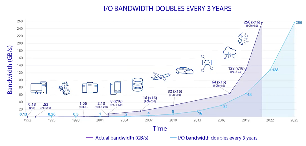
From PCI 1.0 introduced in the 90’s at speeds of 130 MB/s, the bandwidth has been doubling every three years. Next came PCI Extended (PCI-X) around 2000, and finally came PCI Express (PCIe) in 2002 with improvements every generation. Current PCIe Gen 5.0 is able to achieve 4GB/s per lane in each direction, giving 64 GB/s over all x16 lanes in the single direction, or in total 128 GB/s of staggering bandwidth.
PCIe topology
I covered this in a previous blogpost on DMA explained but to reiterate. The Root Complex is an entity that includes a Host Bridge and one or more root ports.
A host bridge (AKA north bridge/memory controller hub) converts processor transactions to PCI transactions, if any memory/IO write is not claimed by another agent (e.g. memory, memory mapped CPU components, legacy devices, etc).
The bridges ‘bus’ and ‘subordinate bus’ describe the bus number ranges they forward TLP packets to. Example endpoint devices can be seen in green below, and Nvidia for example has two BDF’s with different Functions on the same device.
A Bus/Device/Function (BDF) forms a hierarchy based addressing scheme. Whilst the Bus and Device are physical concepts in the device, the Function allows for logically independent components in the physical device. Hence a BDF represents a unique component in the system.
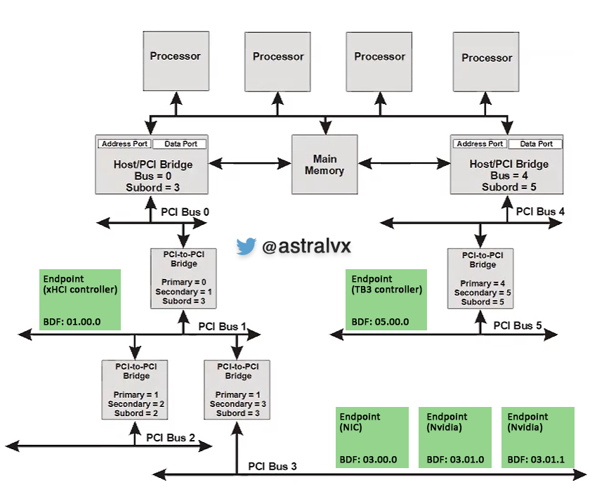
As a note – there is only a maximum of 256 buses supported, and current technology i.e. building giant arrays of disks using PCI can quickly consume all your buses. Thus the creation of ‘PCI Segments’, where a B.D.F is not enough to access a device. But prepending the transaction with a segment i.e. 00.03.00.1, described later.
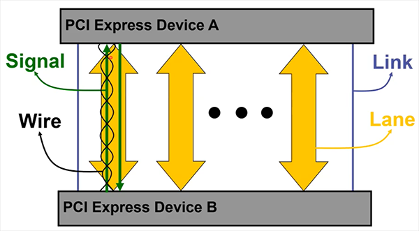
PCIe devices connect to each other via virtual links, where each lane has a wire/signal (RX/TX) and each link can have multiple lanes.
Transaction types
In PCIe there four types of transaction:
- I/O read or write – used to transfer data to a target device via CPU IO port
- Memory read or write – used to transfer data to a target device via MMIO
- Configuration read or write – used to discover device capabilities, program features, and check status of the target device
- Messages – used for event signalling
PCIe spec docs
Base specifications contains the – Software layer. Transaction layer. Data Link layer. Physical Layer.
Form factor specifications contains the – Mechanical layer (CEM card, MiniCEM, M.2, cable, OCuLink)
Configuration Address Space
Setup by both the firmware of the device and software (BIOS/OS). It allows configuration and control of PCI devices where each is assigned a unique Configuration Address Space that will not conflict with others. This also allows for supporting Plug-And-Play (PNP) devices within the OS.
This Configuration Address Space is accessible via:
- Configuration Access Mechanism (CAM) – PCI legacy method using I/O ports 0xCF8 (32-bit configuration address to access) and 0xCFC (data to and from the access). This method only supports 256 buses, each with up to 32 devices, each supporting 8 functions, and assumes use of PCI Segment 0. Either do it in x86 using the OUT instruction or use compiler intrinsic __outbyte(port, data).
- Enhanced Configuration Access Mechanism (ECAM) – PCIe supports access to device configuration spaces via a memory mapped address range, and ECAM support devices extends the config space from 256 bytes to 4096 bytes. ECAM also introduces PCI Segments, allowing more than 256 buses to be accessible by the CPU.
Using the legacy CAM method for example to access config space of an Nvidia video card device on BDF 03.00.0 and read the DeviceId at register 0x4, we could would construct the address like so 80000000h | 03h << 16 | 00h << 11 | 0h << 8 | 4 giving us 80030004h.
Using the ECAM method, we could access config space proprietary register 0x500 of a Nvidia card at BDF 03.00.0 by (assuming no cached device tree) first checking the MCFG ACPI table, choosing the correct ECAM entry corresponding to PCI Segment the device lives in, in the ECAM struct locating the system physical address for the ECAM base address (e.g. F0000000h), then getting to the BDF offset via F0000000h + (03h << 20 | 00h << 15 | 0h << 12 | 500h) giving us the system physical address of the 4K config space accessing offset 0x500 of the Nvidia card at 00000000_F0300500h. This is easily validated by using windbg physical memory display !db.
kd> !db 00000000F0300500
f0300500 18 80 6c 00 85 06 18 1c-00 01 02 00 dd 00 70 04
f0300510 c0 35 18 18 04 b1 15 00-16 a0 00 00 0a 20 14 3c
[..]
The image below shows the standard 64 Byte registers in the 256 Byte config space header. Using ECAM this is extended to 4 KiB, but for backwards compatibility the first 64 bytes are the common header.

- VendorID = PCI-SIG assigned
- DeviceID = vendor self assigned
- Subsystem VendorID = PCI-SIG assigned
- Subsystem DeviceID = vendor self assigned
- Address decode controls
- Software i.e. firmware, OS, read and writes BARs to determine size required and maps into system memory as needed
- Memory, I/O, and bus master enables
- Capabilities List – linked list about features e.g. power management, PCI-X, PCIe, custom, etc
- Interrupts – explained below
OS loads kernel driver based on the VendorID and DeviceID when enumerating PCI devices on the PCI bus. A driver INF will typically contain hardware ID and Windows matches this with config space findings.
BAR
Base Address Register (BARs) are Memory Mapped I/O (MMIO) which means they occupy some of the system address space, not as regular memory but as device I/O.
The system address space can be thought of as a numerical field than you can allocate parts to something. Mostly it’s from main memory, but it also contains memory on the device itself accessed through hardware registers.
From within the OS reading a MMIO region, the Memory Controller will first check if the target address is part of DRAM, if it’s not claimed then the transaction can be converted to a PCI transaction and sent down the PCI bus. Where PCI device decoders will check every packet sent to it and determine if they need to respond, from the OS’s point of view it will get back the memory read regardless of where it was obtained.
Interrupts
PCI introduced INTx, which are INTA#, INTB#, INTC#, INTD#. They are level sensitive, decoupled from CPU interrupts, system controlled INTx to CPU interrupt mapping via physical wires on the mainboard to the CPU. INTx have to remain asserted (high voltage applied) until the CPU processes the interrupt.
Modern PCIe devices uses Message Signaled Interrupt (MSI) and MSI-X. It replaces the previous INTx wire/message with a memory write scheme, and does not require a continuous assertion, but a single message signal is enough for the processor to hold that interrupt in a queue until a kernel driver processes the interrupt. MSI is a single address scheme, but MSI-X allows for 2048 interrupts, so a single device can have multiple different message interrupt signals handled differently by the OS software.
MSI-X gives OS more control by allowing each interrupt vector to have its own address and own data value, thereby giving OS flexibility and control to avoid collisions unlike with INTx where the hardware devices control their interrupt vector.
PCIe speed evolution
To meet the rising demands of speed, cost, and power inter-connectivity PCI-SIG continues to evolve the PCIe architecture, which is looking at PCIe Gen 6.0 to achieve 256 GB/s total transfer. At these sorts of speeds the laws of macro physics come into play and start causing jitter and other electrical issues on the line.
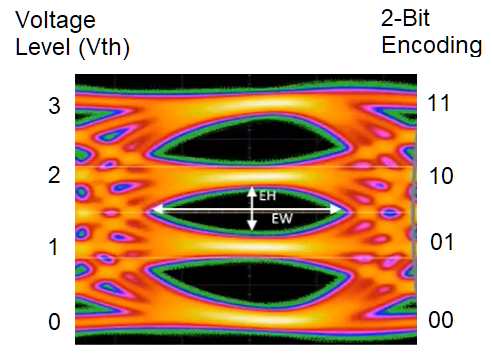
A novel approach has been developed by PCI-SIG to actually allow for these extremely high speeds. Using Pulse Amplitude Modulation 4-level signalling (PAM4), there are now 4 levels (2 bits) per clock cycle. Thus every tick giving you 0, 1, 2, 3 instead of just 0 or 1. In the image below you see 3 black eyes, giving the 4 different voltage levels unlike just 1 eye (for 0 and 1). This was done by reducing the voltage levels Eye Height (EH) and Eye Width (EW), which both increase the susceptibility to errors.
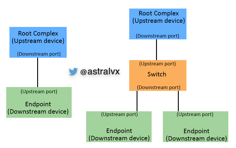
Upstream and downstream port
When reading the PCIe spec and such you will across the term upstream and downstream port often. Even viewing PCI devices in Windows device manager you’ll see these terms.
It’s all about the perspective. Relative to the root, upstream is towards the root, and downstream is away from the root. If the device is a switch, then the perspective is from the switch to determine which is the up/downstream port.
Additional features
PCIe has lots of error handling builtin to the spec and since it’s all hardware based it is very performant. From Data Integrity to Error Handling accross:
- Link level – LCRC
- Link level – ACK/NAK
- End to end – ECRC
- Advanced power management and OS is aware of states D1, D2, D3
PCIe Segments
As mentioned in the ‘PCIe Topology’ chapter before, the 256 bus limit is starting to cause road blocks for systems. PCI segments are a logical software concept, but it has hardware instantiation. In legacy PCI as mentioned you could access config space via bus:dev:fun:offset, but using PCIe it’s automatically defaulted to use PCI segment 0 to support backwards compatibility with PCI.
PCI segments typically originate from the host bridge. So a CPU could have multiple host bridges, but more likely you’ll find e.g. servers with multiple CPU sockets, since each CPU has their own host bridge, thus multiple PCI segments in this platform as there is a PCI segment for each host bridge. Typically there is still only a single IO Controller Hub (south bridge), even with multiple sockets.
However in modern system our BIOS and OS software should access config spaces via segment:bus:dev:fun:offset, because as we move into the future we are starting to approach platforms using nearly all 256 buses on Segment 0. Servers with raid controllers especially can reach this scenario, but even regular notebooks and desktops could have docks with 20 ports and consume 20+ buses, or fancy graphic cards with AI enabled and built-in FPGA all consuming dozens of buses.
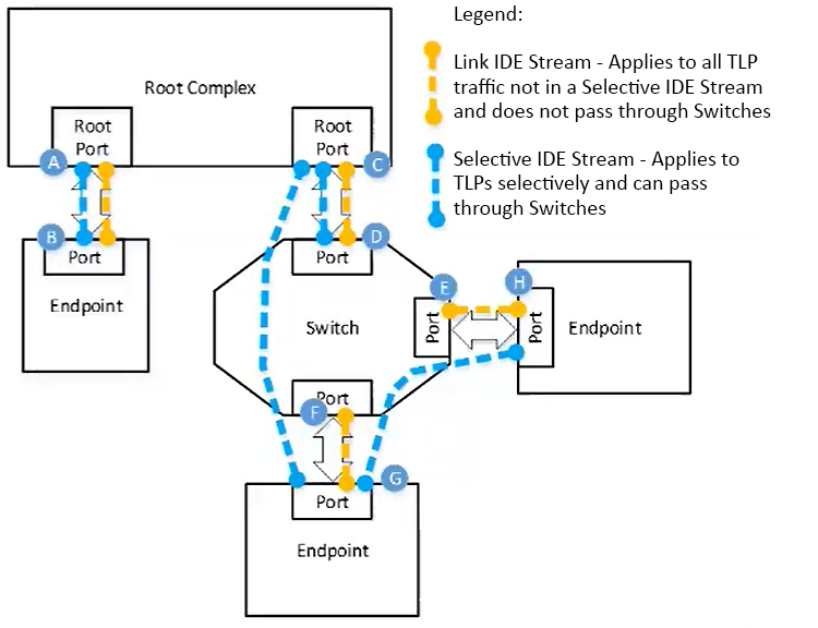
Link level encryption
Coming in PCIe 6.0 is link level encryption to protect against physical attacks, prevent reading of data, preventing modifying/deletion of TLP’s.
Link IDE is encrypted from port to port, and Selective IDE can direct from 1 port to another without encrypting with intermediary switches.
AES-GCM is used as the encryption for the TLP Data Payload.