Disclaimer: it’s a 3.9 MB Linux kernel ; )
N.b. whilst I will try to explain concepts to those new to this field, this blog assumes a lot of fundamental knowledge on FPGAs, RTL development, Vivado, Petalinux, SOC/CPU architecture, memory managers, memory hardware, SPI NOR flash memory, reset vectors, multi-stage bootloaders, kernel device trees, and Linux kernel internals.
Introduction
In this blogpost we’ll be building a stripped down embedded Linux Kernel using Xilinx Petalinux, with a First Stage Bootloader (FSBL), U-boot as a second stage bootloader, and a stripped down RAM-based file system (initramfs). We will be targeting a low end FPGA, the Nexys A7 100T with 128 MB DDR2, 16 MB SPI NOR flash, a bare-metal soft-core embedded Microblaze (RISC) processor, running a system clock of 100 MHz, DDR2 memory clock at 200 MHz, and core FPGA logic and Linux kernel running at 75 MHz to meet timing.
Hardware Design
This hardware design in Fig 1 was created in Vivado Block Design with custom RTL. It is a MicroBlaze (RISC-based) FPGA SoC with PLL‑driven DDR2 memory. It includes 128 KB BRAM, GPIO, Timer, UART, and Quad SPI (QSPI) Flash on an AXI interconnect with interrupt and debug modules. A synchronous reset from the processor system reset, LED15 indicates DDR calibration, and a Blinker RTL confirms logic operation – forming a complete Petalinux hardware platform. More hardware design details on signals, RTL, IP blocks below.
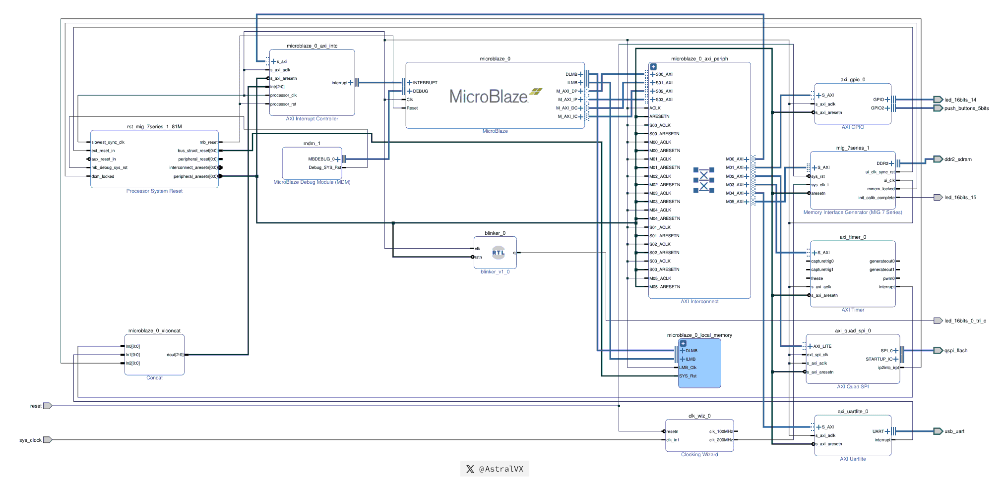
- Active low
reset sys_clockrunning at 100 MHzSys_clockinput drives theClocking WizardIP, which instantiates a PLL generating a 200 MHz clock- A
Memory Interface Generator(MIG) that connects to my 128 MB DDR2 SDRAM, asserts LED15 when initialization calibration is complete, is fed by the 200 MHz clock, and using an internal PLL generates a 75 MHzui_clkultimately used as the main clock for the rest of the design - A
Processor System ResetIP synchronously manages the de‑assertion of reset. Its outputperipheral_aresetnis used as the reset signal for most IP blocks. TheMicroblaze_0_local_memoryis instead driven by the slowerbus_struct_reset, while theMicroBlazeprocessor core itself is driven bymb_reset, the slowest resetn signal, ensuring all other IP blocks have already come out of reset before the processor starts MicroBlazeis a 32‑bit RISC soft‑processor core, “soft” meaning it is implemented entirely in FPGA logic (LUTs, registers, and BRAM). In contrast, high‑end FPGAs may include hard-processor cores, which are dedicated, pre‑fabricated silicon blocks capable of running at much higher clock frequencies. More details on our MicroBlaze IP laterMicroblaze_0_local_memoryis the (Block RAM) BRAM of 128 KB, used by bootloaders for pre-DDR temporary volatile storage. BRAM is small, fast, dedicated on-chip memory with 1 cycle latency (10ns @ 100 MHz), unlike DDR which often has 160 ns access times- Then we have numerous IP blocks accessed over Advanced eXtensible Interface (AXI) buses. AXI is used for data paths between IP modules and is widely used and straightforward to implement in both the FPGA and ASIC world.
AXI GPIO: controls LED14 and five push buttonsAXI Timer: generates the system timer tick as an interrupt for the Linux kernel.AXI Quad SPI: interfaces to a 16 MB NOR SPI Flash where we store the FPGA bitstream, First Stage Boot Loader (FSBL), U‑Boot, U‑Boot script, and other firmware. More details on the Flash layout are given laterAXI Uartlite: provides a simple serial communication interface between the soft‑core processor and the host machine running PuTTY, used for printing boot logs during debugging and for interactive FSBL/U‑Boot command‑line promptsAXI Interconnect: acts as a central switch that routes memory‑mapped transactions between the soft‑core processor (master) and the IP cores (slaves), enabling them to share a common bus architecture. It also handles Clock Domain Crossing (CDC) between different clock domains, i.e. DDR2 at 200 MHz and MicroBlaze at 75 MHz. It ultimately defines the system address map, which many of you familiar with OS internals will recognize. More on this later.
Concat: a simple IP module that combines three interrupts (AXI Timer, AXI Uartlite, AXI Quad SPI) into a single bus, which is fed into the ‘AXI Interrupt Controller’AXI Interrupt Controller: an IP core that manages the priority of multiple interrupt sources and presents them as a single interrupt request (IRQ) to the MicroBlaze interrupt pinMicroBlaze Debug Module: enables JTAG-based software debugging, including hardware breakpoints, watchpoints, and memory access, for the MicroBlaze soft-processor. It acts as a bridge between a debugger (e.g. XSDB) and the processorBlinker_0: custom RTL that blinksled_16bits_0_tri_oonce per second, so I can be certain that the FPGA core logic is running correctly. RTL below for those interested.- All external pins on the left are signal inputs (
reset,sys_clk), and those on the right are bi-directional outputs driving external interfaces (ddr2_sdram,usb_uart,qspi_flash,led_16bits_15, etc)
module blinker(
    input  wire clk,
    input  wire rstn,
    output wire q
);
    localparam integer TERMINAL_COUNT = 75_000_000 - 1; // 75 MHz, 1 sec
    reg [26:0] count = 27'd0;
    reg        q_reg = 1'b0;

    always @(posedge clk or negedge rstn) begin
        if (!rstn) begin
            count <= 26'd0;
            q_reg <= 1'b0;
        end
        else begin
            if (count == TERMINAL_COUNT) begin
                count <= 26'd0;
                q_reg <= ~q_reg;      // Toggle every 1 second
            end
            else begin
                count <= count + 1'b1;
            end
        end
    end

    assign q = q_reg;

endmodule
Implementation Schematic
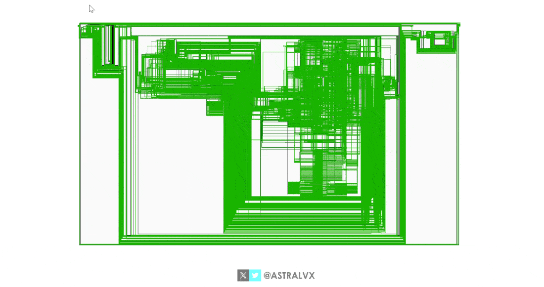
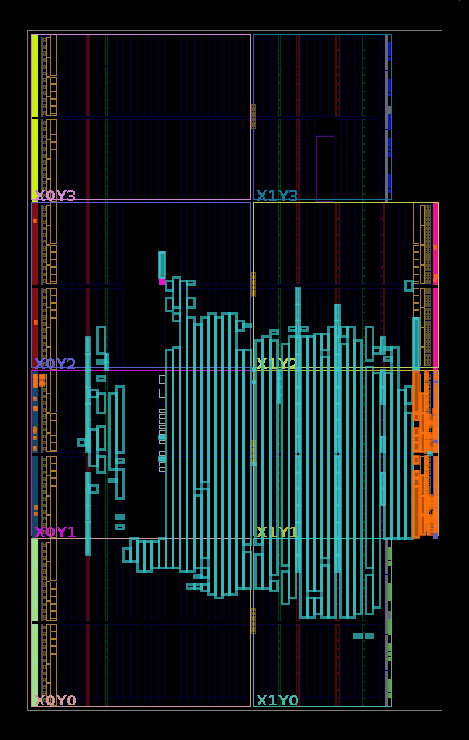
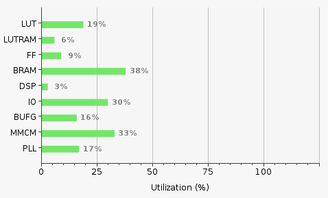
Later on in the blogpost, when I refer to the FPGA bitstream configuring its resources this is what I am referring to. Fig 2 as a GIF shows the hardware design logically as a schematic view (after implementation), this is the post-synthesis netlist – a logical diagram of LUTs, FFs, and FPGA primitives with their interconnections, but not tied to specific physical locations on the chip. Notice the initial large central chaos is my Microblaze processor. Whereas Fig 3 and 4 shows the Device view after implementation (placement, routing of netlist), it shows the chip floorplan, i.e. the actual physical layout of our design mapped onto the target FPGA die. It shows LUTs, FFs, DSPs, BRAMs placed in CLB sites; routing tracks show physical interconnects between placed elements; and resource utilization of slice usage, I/O banks, clock regions, MIG/DDR placement, etc. Successfully met timing with 0.875 ns slack running at a core 100 MHz clock.
System Address Map
In Fig 5 below we see our System Address Map (this is different from the OS Memory Map), it is the entire system’s logical address space (CPU-visible), mapping peripherals, logic IP cores, and DDR.
This is accessed via Vivado Address Editor, and entries are correlated to modules seen previously in Fig 1. I have manually assigned memory-mapped addresses to IP blocks (slaves) connected to the processor (master) to fit in a 32-bit System Address space. I could have chosen a smaller address space, however my Microblaze processor operates at instruction and data widths of 32-bits, so I get this full 32‑bit address space without additional cost from the compute engine.

AXI
By using AXI compatible IP blocks we abstract away the complexity of the underlying hardware. Instead of me gruelingly writing the RTL for a memory controller with the incredibly complex state machine and command pipeline, or writing the RTL for a Quad SPI controller handling the bus lines and opcodes and data and errors, or writing the RS232 serial protocol for UART. I can instead use Xilinx provided IP that is AXI compatible, since Xilinx has wrote RTL for hundreds of IP blocks, they did the testing, and made sure it’s “robust”. Hence I can focus on my design, without all of this it would have been impossible for me to complete this POC. Due to IP licensing fees, in the real world FPGA and ASIC engineers develop the protocol from the ground-up.
N.b. AXI is a standardized bus protocol for FPGAs and ASICs, it deals with handshaking between transactions, supports burst mode (i.e. setup transaction config in 1 cycle, then all subsequent cycles are data cycles, used extensively in DMA for high throughput), supports 5 independent channels for r/w of addresses and data, can support differing use-cases from streaming data to full fledged memory mappings. So if your Quad SPI controller is AXI compatible, there is IP helpfully doing protocol translation from SPI cycles to standard AXI cycles.
DDR2 Memory
DDR2 memory of 128 MB is at address 0x8000_0000 to 0x8FFF_FFFF, so from Linux this is the address range to read/write to this volatile RAM. The 16 MB SPI Flash is located at 0x4500_0000, so if you want to read say offset 0x1000 in Flash, from the Linux kernel read system address 0x4500_1000, and under the hood the SPI protocol cycles will be generated and data returned to you over the standard AXI bus. To read and write from push buttons and LEDs, the GPIO space is at 0x4000_0000, of course 64 KB is a bit much for 6 bits worth of signals haha. At address 0x0000_0000 I have my 128 KB of BRAM, the ultra fast, low-latency scratchpad memory (this is not equivalent to L1 cache on CPUs, instead L1 cache would be equivalent to my 32 KB instruction cache and 32 KB data cache talked about later). Since I have don’t have any memory protection in the form of IOMMU etc, a Linux user could easily cause havoc by writing to the timer register space at 0x41C0_0000, but this is a POC.
PetaLinux
Petalinux is a customizable embedded Linux-based system provided by Xilinx for their FPGAs and SoC devices. It creates a Board Support Package (BSP) that contains the hardware platform, bootloaders, device tree, kernel config, etc, allowing a developer to boot a physical board with a Linux system, in our case the FPGA with all its hardware components. It has a very high learning curve because it sits at the complex intersection of FPGA hardware design, Linux kernel development, and Yocto-based build systems. It requires a lot of hand holding to build things as expected, ineffective documentation, bugs with every new version, where you have to build your own Yocto recipes or manually patch binaries to workaround their issues. For all it’s downsides, it creates highly customizable and streamlined Linux systems. Key commands are:
petalinux-create  // Generates a new PetaLinux project
petalinux-config  // Configures the project system settings, kernel (-c kernel), root filesystem
                  // (-c rootfs), and U-Boot (-c uboot), you will spend a lot of time in here
petalinux-build   // Builds the system image, including hardware-specific components
petalinux-boot    // Boots images using JTAG, useful for quick testing
petalinux-package // Packages images for boot, i.e. creating BOOT.BIN to be flashed into SPI Flash
petalinux-devtool // Manages user-defined code (recipes) within the PetaLinux environment
Files created by Petalinux for my BSP are:
fs-boot.elf  // First-stage bootloader, extracted from hardware design (.XSA) that is exported from Vivado
system.bit   // FPGA bitstream, it gets shifted into FPGA configuration logic during boot by JTAG or FSBL
download.bit // Single binary that merges the hardware design system.bit and first-stage bootloader

u-boot.elf   // U-boot image (second-stage bootloader) in ELF format, loaded into DDR by JTAG or FSBL
u-boot-s.bin // Raw u-boot binary, wrapped with Microblaze specific headers, used by BOOT.bin for Flash loading
boot.scr     // U-Boot script binary that tells bootloader how to load kernel, device tree, root filesystem into memory

rootfs.cpio.gz.u-boot // A compressed initial RAM disk (initramfs) Linux root filesystem
system.dtb   // A compiled Device Tree Blob (DTB), describing hardware components to the kernel (i.e. CPU, arch, memory, peripherals)
image.ub     // A Flattened Image Tree (FIT) image, single packed binary containing Linux kernel, above root filesystem, and above device tree

BOOT.bin     // The primary boot image used by Xilinx FPGA/SOCs, contains all of the above (mine is currently 15.3 MB), stored in SPI flash
Flash layout
Using the above PetaLinux configurations and after several weeks of development, debugging, and troubleshooting, I finally succeeded in booting a Linux kernel booting from QSPI. Fig 6 below shows the final flash layout for my 16 MB SPI. These fixed partition sizes give a little bit of wiggle-room if the binaries grow, overall all 16 MB is consumed, and it was painful removing U-boot packages, rootfs packages, and kernel modules, to make it fit into 16 MB while keeping the system functional.
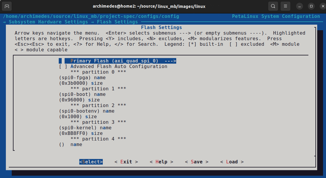
Spi0-fpga partition
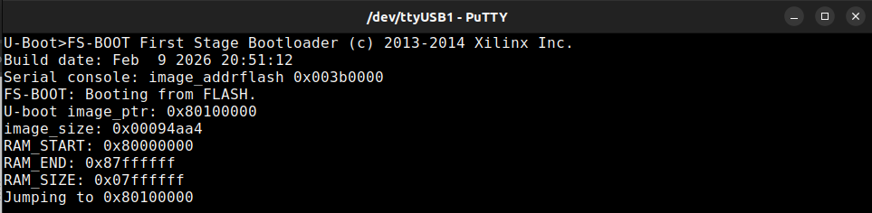
Contains the file download.bit, which the petalinux-build command creates. It is composed of system.bit (FPGA bitstream exported from Vivado) and fs-boot.elf (first-stage bootloader). Fs-boot log can be seen in Fig 7, and fs-boot.elf can be configured using commands:
petalinux-devtool reset fs-boot   // Clear out caching issues
petalinux-devtool modify fs-boot  // Extracts out the source code from the Yocto recipe for Microblaze FSBL
// Modify linux_mb/components/yocto/workspace/sources/fs-boot/lib/sw_apps/mba_fs_boot/src/fs-boot.c
// N.b. my root folder for this project, the Board Support Package (BSP) is linux_mb/
petalinux-build -c fs-boot        // Build fs-boot.elf
Spi0-boot partition
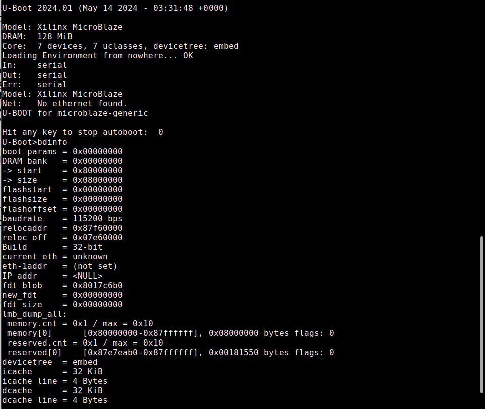
Contains U-boot-s.bin our second-stage boot loader. Configuration of U-boot is scattered over the petalinux-config and petalinux-config -c u-boot . An important value is the Text Base, mine set to 0x8010_0000, FSBL will write U-boot into this memory address and execute it. You can interact with the U-boot prompt for live debugging, either by loading the full BOOT.bit or simply petalinux-boot jtag --fpga which will loads all relevant binaries into memory until U-boot. Fig 8 below shows my U-boot log, and issuing the bdinfo command to print board information, shows my 32-bit processor architecture, DDR2 of 128 MB starting at 0x8000_0000 and ending at 0x8800_0000, the relocaddr where U-boot will be relocated to when the kernel loads, and instruction/data caches of 32 KB each.
Spi0-bootenv partition
Contains the U-boot script boot.scr that U-boot will execute. It is created when you run petalinux-package and lives under linux_mb/images/linux. The script contains the U-boot commands to set environment variables, copy from SPI Flash the Linux kernel (image.ub), device tree, and root filesystem into memory into addresses specified by Petalinux configurations. Below is my U-boot binary script to download, and important parts for execution are:
– Lines 13-14 for JTAG execution of the kernel – boot kernel at 0x86000000, using ramdisk at 0x87000000, and device tree at 0x87f00000
– Lines 55-57 for QSPI execution of the kernel – SPI Flash read kernel offset 0x447000, size 0xBB8FF0, and write into memory 0x8600_0000, then boot it
N.b. for JTAG, the Petalinux tool XSDB on the host side downloads those 3 images into the FPGAs DDR2 memory over JTAG before U-Boot runs, and for QSPI they are loaded by the FSBL from Flash
if test "${boot_target}" = "jtag" ; then
    run update_bootargs
    bootm 0x86000000 0x87000000 0x87f00000
    if test "${boot_target}" = "xspi0" || test "${boot_target}" = "xspi1" || test "${boot_target}" = "qspi" || test "${boot_target}" = "qspi0"; then
        sf probe 0 0 0;
        sf read 0x86000000 0x447000 0xBB8FF0
        bootm 0x86000000;
        echo "Booting using Fit image failed"
Spi0-kernel partition
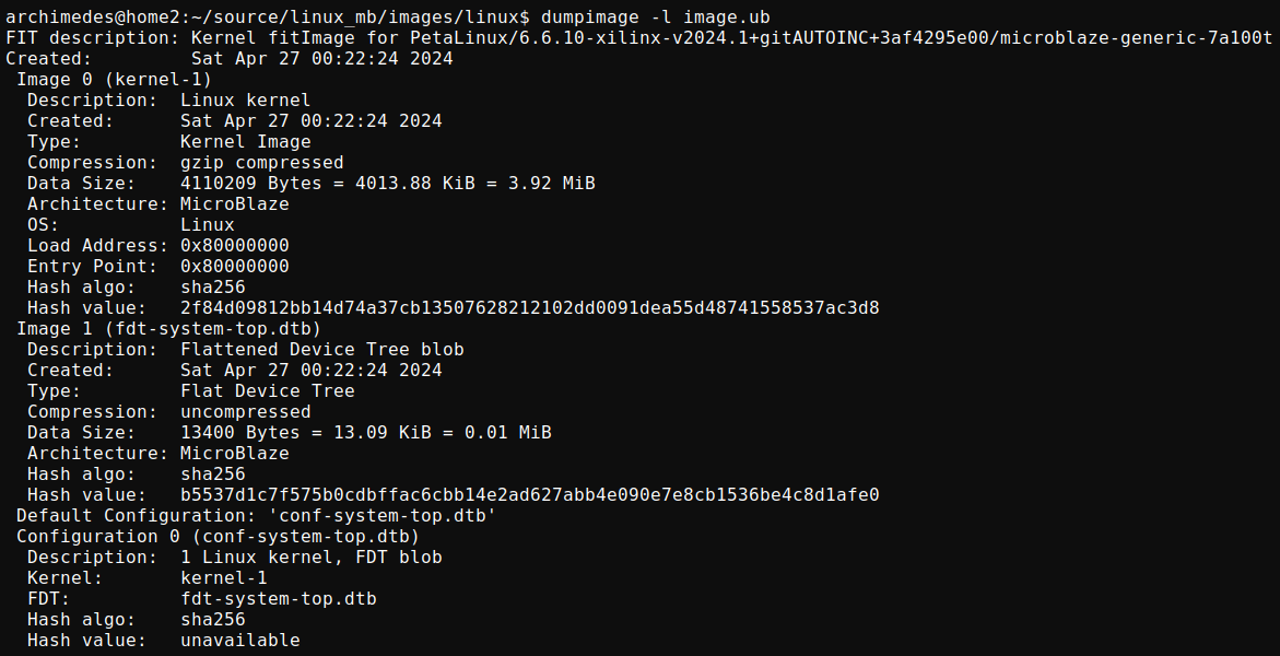
The last partition contains image.ub a FIT image. This image is a packed binary consisting of the Linux kernel compiled for my Microblaze RISC architecture, a root filesystem (initramfs), and the system device tree (all hardware presented to kernel). Configuration for the kernel is spread over petalinux-config and petalinux-config -c kernel. A lot of device drivers are disabled, from PCI support, to all networking except ethernet, only EXT4 file system supported, most debugging disabled apart from the core logs, most security features are disabled, all cryptography routines are disabled except AES, MD5, SHA2, and CRC32, disabled DMA, and so much more. This leads to this incredibly tiny size of 3.9 MB, by using imagedump for analysis seen in Fig 9.
N.b. Petalinux bug around created date
N.b.b. dumpimage issue not finding the INITRAMFS root file system packed
N.b.b. notice my processor architecture is Microblaze RISC from my hardware design in Vivado, usually you would see ISAs like x86_64/ARM/RISC-V etc.
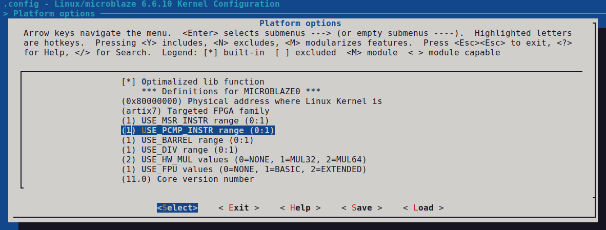
Opening the kernel config in Petalinux, and choosing Platform options as seen in Fig 10 below shows my simple Microblaze processor execution units for use by the kernel, it includes (MSR-related instructions, barrel shifter, divider, multiplier, FPU, special instructions, etc). The System Device Tree contains the complete feature set of my processor.
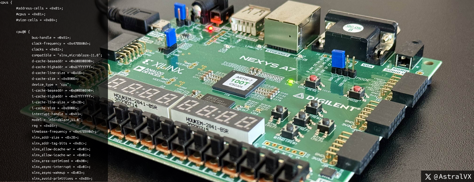
System Device Tree
As mentioned image.ub contains the System Device Tree typically used by ARM/RISC-V/embedded systems, this system.dtb binary blob can be read using a device tree decompiler: dtc -I dtb -O dts system.dtb -o system.dts
The resulting Device Tree is very large, but it fully describes the hardware components of the system, this is similar to Windows and UEFI-BIOS ACPI tables (i.e. DSDT, SSDT) which are the (Intel/AMD) x86 standard for hardware discovery on Windows systems.
I can’t explain the entire file, but I will comment on some interesting points:
cpus { cpu@0 } // Single-core Microblaze system
clock-frequency = <0x478860d>; // Clock frequency runs at 75.007501 MHz
interrupt-handle = <0x03>; // Interrupt controller handles 3 interrupts
xlnx,async-interrupt = <0x01>; // Asynchronous interrupts coming from different clock domains
interrupt-is-edge = <0x00> // Interrupts are level-sensitive
num-sync-ff-clk-irq = <0x01 // Interrupts have 1 synchronizer FF to handle clock domain crossing
xlnx,d-axi = <0x01>; // Processor core uses AXI4 bus for data paths (connecting DDR2 to other peripherals, memory traffic load/store instructions hitting the D-cache or bypassing it)
d-cache-size = <0x8000>; // Data cache line is 32 KB
xlnx,dcache-line-len = <0x04>; // Sets data cache line length to 4 words (16 bytes), controls how much data is fetched from DDR on a cache miss
xlnx,dcache-use-writeback = <0x01>; // Enables write-back caching mode for the D-cache, modified ("dirty") cache lines stay in cache until evicted
xlnx,debug-enabled = <0x01>; // Enables the MicroBlaze Debug Module (MDM) interface on the core, allows for JTAG debugging via XSDB to set breakpoints, single step, register inspection, write to memory
xlnx,endianness = <0x01>; // Configures the MicroBlaze core as little-endian
xlnx,mmu-dtlb-size = <0x04>; // Sets the data TLB size to 4 entries (fully associative).
xlnx,mmu-privileged-instr = <0x00>; // Disables privileged mode instructions (no user/supervisor mode separation).
xlnx,opcode-0x0-illegal = <0x01>; // Generate illegal opcode exception on executing 0x00000000
xlnx,use-mmu = <0x03>; // Enables a full MMU with both instruction and data virtual to physical memory translation
memory@80000000 //  Linux's physical memory address for the kernel memory map
gpio@40000000 // GPIO dual-channel controller at base address 0x40000000, controlling LED15 and 5x push buttons, with tri-state disabled
[..]
Root filesystem (RAM based)
As mentioned image.ub contains the root filesystem (INITRAMFS), which is a small, compressed CPIO archive loaded into memory by the bootloader, providing a temporary root filesystem that allows the Linux kernel to boot. To fit this into my 16 MB SPI Flash, I used a Yocto recipe petalinux-image-minimal which strips downs initramfs to contain only essentials for Linux to boot and run basic commands:
- BusyBox (combined coreutils: ls, cat, mount, etc)
- Basic device drivers for my hardware and their interrupts (UART, GPIO, timer)
- Minimal kernel modules for MIG DDR and AXI hardware peripherals
- No GUI, package manager, or bloat
FPGA boot sequence from SPI Flash
The boot flow of my system in short is:
> Read QSPI NOR (bitstream, FSBL/U‑Boot, images)
> FPGA fabric configuration for MicroBlaze, peripherals, BRAM preloaded with the FSBL, bring up MIG DDR2 (done = LED15)
> MicroBlaze processor boots from BRAM, executes reset vector
> MicroBlaze copies First stage bootloader from BRAM into DDR
> First stage bootloader sets up clock, memory, and loads images from SPI into DDR
> Second stage bootloader (U-boot) setup bootargs, kernel, initramfs, device tree
> Linux kernel, sets up memory management unit, drivers initialize from the device tree
> Minimal rootfs gives us a small MicroBlaze Linux environment on top of our custom FPGA SoC
- Power-on reset. Nexys A7 (xc7a100t chip) starts in Shift Configuration Data state. Internal CCLK (Configuration Clock) begins toggling at a fixed few MHz from internal oscillator.
- Hardcoded state machine (etched into silicon) samples the physical dip switch to set boot mode. It finds QSPI (Master SPI x4 mode).
- Hardcoded silicon Quad SPI controller reads NOR Flash physical address 0x0 (BOOT.bin). At bytes 0x0 – 0x8 is the Flash offset to the FPGA bitstream.
- Hardcoded silicon configuration state machine reads the bitstream packets and configures the FPGA’s fabric to instantiate hardware:
- CLB LUTs/FFs: MicroBlaze processor, Blinker RTL
- BRAM: MicroBlaze local memory (128 KB), automatically initialized with FSBL as part of Vivado design
- PLL: Clock wizard (sys_clock at 100 MHz, MIG internal DDR PLL at 200 MHz, ui_clk output from MIG at 75 MHz)
- I/O blocks: DDR2 SDRAM, USB UART, QSPI Flash, LEDs
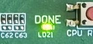
- LED DONE is set when Bitstream configuration is complete, and LED15 is set when MIG DDR2 has completed calibration
- MicroBlaze runs reset vector at BRAM 0x00000000, this is where the First Stage Bootloader resides.
- FSBL starts executions and relocates itself from BRAM into DDR2 memory.
- FSBL then initializes the main clock of 100 MHz.
- FSBL performs DDR2 read/write tests and peripheral self-tests (UART, timer, GPIO).
- FSBL performs QSPI reads of the Flash partitions, and copies U-boot / U-boot script / Kernel and DTB into DDR2 memory at their predetermined addresses.
spi0-boot:    U-Boot            (DDR 0x80100000)
spi0-bootenv: U-Boot env/script
spi0-kernel:  Linux kernel      (DDR 0x87000000)
Device Tree Binary:             (DDR 0x87f00000)
- FSBL lastly hands off execution to the second stage bootloader (U-boot). Refer back to Fig abc, and notice
uart_print("Jumping to 0x80100000"); - U-boot runs from DDR2 at 0x8010_0000, runs its boot script, and parses the device tree in memory. It discovers peripherals during its own operation, and will pass these onto the kernel later.
U-Boot> spi device 0:0
4000000  10000 0 axi_gpio_0 @0x40000000
40600000 10000 0 axi_uartlite_0 @0x40600000
41200000 10000 0 axi_intc @0x41200000
- U-boot creates the kernel bootargs, ours is simple – set main console device as ttyUL0 (AXI UARTLite peripheral in our FPGA design), set baud rate to 9600 bps, enable very early console output via printk().
(console=ttyUL0,9600 earlycon)
- U-boot then runs the final command from boot.scr where it reads the kernel from Flash offset 0x447000, size 0xBB8FF0, and writes into memory 0x8600_0000, then boot it.
sf read 0x86000000 0x447000 0xBB8FF0
bootm 0x86000000
- The (MicroBlaze architecture) Linux kernel uncompresses and starts, using the passed device tree to discover:
- CPU features (MMU, caches, FPU, MSR/PCMP, debug, etc)
- 128 MB of RAM at 0x8000_0000
- AXI UART, GPIO, Timer, SPI, Interrupt Controller, and MIG nodes
MMU, kernel page tables, Microblaze TLB, caches
- Kernel sets up the Memory Management Unit (MMU) for our Microblaze architecture since we defined it in DTS as:
xlnx,use-mmu = <0x03>. This then enables:- Unified TLB (UTLB) – larger, software-managed cache that stores both instruction and data page translations
- Instruction TLB (ITLB) / Data TLB (DTLB) – smaller, faster, hardware-managed caches that “shadow” the most recently used translations from the UTLB to reduce latency
- Virtual Address – MMU translates Virtual Addresses (used by Linux) to Physical Addresses (used by hardware), the TLBs store these mapping results
31             22 21           12 11                0
+-- VPN[31:22] --+- EPN[21:12] --+-- Offset[11:0] --+
| Kernel virtual | Huge page   | Page offset        |
| 0xC000_0000    | (2MB pages) | (4KB pages)        |
+----------------+-------------+--------------------+
- Kernel sets up initial page tables for the MMU, configures ITLB and DTLB to device tree values:
mmu-itlb-size=<0x02>, mmu-dtlb-size=<0x04>which means:- UTLB:
[31:22] Effective Page Number (EPN) i.e. VA[31:22]
[21:10] Real Page Number (RPN) i.e. PA[31:12] base
[ 9: 2] Page size
[ 1: 0] Zone 0=user, 1=kernel (xlnx,mmu-zones=2)
+ PID[7:0] Process ID (protection)
+ C/I/R/W/X Cache/Guard/Exec perms
- ITLB: 2-entry instruction shadow TLB (cache of UTLB for code fetches)
ITLB[0]: EPN=0x80000, RPN=0x80000 (1:1 DDR mapping, kernel zone)
ITLB[1]: EPN=0xC0000, RPN=0x80000 (kernel code virtual-to-physical)
- DTLB: 4-entry data shadow TLB (cache of UTLB for load/store)
DTLB[0]: EPN=0x80000, RPN=0x80000 (128MB DDR, cacheable, writeback)
DTLB[1]: EPN=0x40000, RPN=0x40000 (GPIO/MMIO, uncached, guarded)
DTLB[2]: EPN=0x40600, RPN=0x40600 (UART, device memory)
DTLB[3]: EPN=0x41200, RPN=0x41200 (Interrupt controller)
- Every memory (instruction/data) access will do a TLB lookup process.
E.g. let’s explain an instruction fetch where PC=0x8000_0100
– MicroBlaze processor first checks its ITLBs for a matching translation
– 0x8000_0100 falls within ITLB[0] of EPN=0x80000, not ITLB[1]
– ITLB provides the associated Real Page Number (RPN), i.e. the base of the translated physical page, in this RPN = 0x80000
– MMU then combines it with the page offset (VA[11:0]) to form:Physical = (RPN<<12) ∣ OffsetPhysical = 0x80000<<12∣0x100 = 0x8000_0100// It's a 1:1 translation, VA==PA ( ;
– Permission bits in TLB also checked from the translation (R/W/X, cache/guard flags, zone = kernel)
– CACHE HIT – since this region is cached and executable, the fetch proceeds normally and the instruction word is pulled from I‑cache (32 KB remember from Vivado design)
– CACHE MISS – assuming 32‑bit instruction was not present, CPU would stall and signal a UTLB refetch where MMU issues a burst request to the AXI interface, fetching the instruction from DDR2 through the MIG controller, and the fetched line is then stored in I‑cache for future reuse (cache miss in my design incurs 16 cycles before CPU can retry and fetch).
- UTLB:
- Kernel configures the AXI Timer as the Linux scheduler tick source, wires our three interrupt sources through the AXI INTC to the single MicroBlaze IRQ, and brings up the UART console on ttyUL0.
- Kernel lastly mounts our minimal initramfs as rootfs, so we now have a basic shell with BusyBox, some minitmal utilities, and access to our hardware via:
/dev/ttyUL0– UART Console/dev/timer– Timer/dev/mtd#– SPI Flash access/dev/mtd0 = spi0-fpga partition (bitstream)
/dev/mtd1 = spi0-boot (U-Boot)
/dev/mtd2 = spi0-bootenv
/dev/mtd3 = spi0-kernel
$ cat /dev/mtd2 # Dump U-Boot environment
/sys/class/gpio/– GPIO Access
I.e. GPIO0[0], an output, connects to led_16bits[14] in our Vivado design
For testing we can drive it from the shell:$ ls /sys/class/gpio/
[..] export gpiochip512 unexport
echo 512 > /sys/class/gpio/export # Export GPIO0[0]
echo out > /sys/class/gpio/gpio512/direction
echo 1 > /sys/class/gpio/gpio512/value # LED14 ON
/proc/iomem– I/O Memory Map$ cat /proc/iomem·
00100000-0010ffff : microblaze_0_local_memory # 128KB BRAM
40000000-4000ffff : axi_gpio_0 # GPIO
40600000-4060ffff : axi_uartlite_0 # UART
41200000-4120ffff : microblaze_0_axi_intc # IRQ controller
41c00000-41c0ffff : axi_timer_0 # System timer
45000000-45ffffff : axi_quad_spi_0 # QSPI NOR
80000000-87ffffff : System RAM # 128MB DDR2 MIG
Complete serial boot log
Build date: Feb 7 2026 23:11:42
Serial console: image_addrflash 0x003b0000
FS-BOOT: Booting from FLASH.
image_ptr: 0x80100000
image_size: 0x00094aa4
RAM_START: 0x80000000
RAM_END: 0x87ffffff
RAM_SIZE: 0x07ffffff
Jumping to 0x80100000
U-Boot 2024.01 (May 14 2024 – 03:31:48 +0000)
Model: Xilinx MicroBlaze
DRAM: 128 MiB
Core: 7 devices, 7 uclasses, devicetree: embed
Loading Environment from nowhere… OK
In: serial
Out: serial
Err: serial
Model: Xilinx MicroBlaze
Net: No ethernet found.
U-BOOT for microblaze-generic
Hit any key to stop autoboot: 0
JTAG: Trying to boot script at 87200000
## Executing script at 87200000
Wrong image format for “source” command
JTAG: SCRIPT FAILED: continuing…
SF: Detected s25fl128s with page size 256 Bytes, erase size 64 KiB, total 16 MiB
device 0 offset 0x446000, size 0x40000
SF: 262144 bytes @ 0x446000 Read: OK
QSPI: Trying to boot script at 87200000
## Executing script at 87200000
Trying to load boot images from jtag
Wrong Image Format for bootm command
ERROR: can’t get kernel image!
Trying to load boot images from qspi
SF: Detected s25fl128s with page size 256 Bytes, erase size 64 KiB, total 16 MiB
device 0 offset 0x447000, size 0xbb8ff0
SF: 12292080 bytes @ 0x447000 Read: OK
## Loading kernel from FIT Image at 86000000 …
Using ‘conf-system-top.dtb’ configuration
Trying ‘kernel-1’ kernel subimage
Description: Linux kernel
Type: Kernel Image
Compression: gzip compressed
Data Start: 0x86000114
Data Size: 10859048 Bytes = 10.4 MiB
Architecture: MicroBlaze
OS: Linux
Load Address: 0x80000000
Entry Point: 0x80000000
Hash algo: sha256
Hash value: 293a1a8a4a1b7de0a96b33466af4b68a0c86ac50abe5de98c75cdaf6e8a4b466
Verifying Hash Integrity … sha256+ OK
## Loading fdt from FIT Image at 86000000 …
Using ‘conf-system-top.dtb’ configuration
Trying ‘fdt-system-top.dtb’ fdt subimage
Description: Flattened Device Tree blob
Type: Flat Device Tree
Compression: uncompressed
Data Start: 0x86a5b450
Data Size: 13400 Bytes = 13.1 KiB
Architecture: MicroBlaze
Hash algo: sha256
Hash value: b5537d1c7f575b0cdbffac6cbb14e2ad627abb4e090e7e8cb1536be4c8d1afe0
Verifying Hash Integrity … sha256+ OK
Booting using the fdt blob at 0x86a5b450
Working FDT set to 86a5b450
Uncompressing Kernel Image
Loading Device Tree to 87e77000, end 87e7d457 … OK
Working FDT set to 87e77000
Starting kernel …
Ramdisk addr 0x00000000,
FDT at 0x87e77000
earlycon: uartlite_a0 at MMIO 0x40600000 (options ‘9600n8’)
printk: bootconsole [uartlite_a0] enabled
cma: Reserved 16 MiB at 0x86c00000 on node -1
Linux version 6.6.10-xilinx-v2024.1-g3af4295e00ef (oe-user@oe-host) (microblazeel-xilinx-linux-gcc (GCC) 12.2.0,
GNU ld (GNU Binutils) 2.39.0.20220819) #1 Sat Apr 27 05:22:24 UTC 2024
setup_memory: max_mapnr: 0x8000
setup_memory: min_low_pfn: 0x80000
setup_memory: max_low_pfn: 0x88000
setup_memory: max_pfn: 0x88000
Zone ranges:
DMA [mem 0x0000000080000000-0x0000000087ffffff]
Normal empty
HighMem empty
Movable zone start for each node
Early memory node ranges
node 0: [mem 0x0000000080000000-0x0000000087ffffff]
Initmem setup node 0 [mem 0x0000000080000000-0x0000000087ffffff]
setup_cpuinfo: initialising
setup_cpuinfo: Using full CPU PVR support
wb_msr
pcpu-alloc: s0 r0 d32768 u32768 alloc=1*32768
pcpu-alloc: [0] 0
Kernel command line: console=ttyUL0,9600 earlycon
Dentry cache hash table entries: 16384 (order: 4, 65536 bytes, linear)
Inode-cache hash table entries: 8192 (order: 3, 32768 bytes, linear)
Built 1 zonelists, mobility grouping on. Total pages: 32512
mem auto-init: stack:all(zero), heap alloc:off, heap free:off
Memory: 88552K/131072K available (6359K kernel code, 569K rwdata, 1692K rodata,
201K init, 322K bss, 26136K reserved, 16384K cma-reserved, 0K highmem)
SLUB: HWalign=32, Order=0-3, MinObjects=0, CPUs=1, Nodes=1
NR_IRQS: 64, nr_irqs: 64, preallocated irqs: 0
irq-xilinx: /pl-bus/interrupt-controller@41200000: num_irq=3, edge=0x6
/pl-bus/timer@41c00000: irq=1
clocksource: xilinx_clocksource: mask: 0xffffffff max_cycles: 0xffffffff, max_idle_ns: 25480924186 ns
xilinx_timer_shutdown
xilinx_timer_set_periodic
sched_clock: 32 bits at 75MHz, resolution 13ns, wraps every 28630252025ns
Calibrating delay loop… 37.06 BogoMIPS (lpj=185344)
pid_max: default: 4096 minimum: 301
Mount-cache hash table entries: 1024 (order: 0, 4096 bytes, linear)
Mountpoint-cache hash table entries: 1024 (order: 0, 4096 bytes, linear)
devtmpfs: initialized
clocksource: jiffies: mask: 0xffffffff max_cycles: 0xffffffff, max_idle_ns: 19112604462750000 ns
futex hash table entries: 16 (order: -4, 448 bytes, linear)
NET: Registered PF_NETLINK/PF_ROUTE protocol family
DMA: preallocated 128 KiB GFP_KERNEL pool for atomic allocations
DMA: preallocated 128 KiB GFP_KERNEL|GFP_DMA pool for atomic allocations
audit: initializing netlink subsys (disabled)
audit: type=2000 audit(0.330:1): state=initialized audit_enabled=0 res=1
pps_core: LinuxPPS API ver. 1 registered
pps_core: Software ver. 5.3.6 – Copyright 2005-2007 Rodolfo Giometti
PTP clock support registered
vgaarb: loaded
clocksource: Switched to clocksource xilinx_clocksource
NET: Registered PF_INET protocol family
IP idents hash table entries: 2048 (order: 2, 16384 bytes, linear)
tcp_listen_portaddr_hash hash table entries: 256 (order: 0, 5120 bytes, linear)
Table-perturb hash table entries: 65536 (order: 6, 262144 bytes, linear)
TCP established hash table entries: 1024 (order: 0, 4096 bytes, linear)
TCP bind hash table entries: 1024 (order: 3, 40960 bytes, linear)
TCP: Hash tables configured (established 1024 bind 1024)
UDP hash table entries: 128 (order: 0, 6144 bytes, linear)
UDP-Lite hash table entries: 128 (order: 0, 6144 bytes, linear)
NET: Registered PF_UNIX/PF_LOCAL protocol family
RPC: Registered named UNIX socket transport module.
RPC: Registered udp transport module.
RPC: Registered tcp transport module.
RPC: Registered tcp-with-tls transport module.
RPC: Registered tcp NFSv4.1 backchannel transport module.
PCI: CLS 0 bytes, default 32
workingset: timestamp_bits=30 max_order=15 bucket_order=0
Key type cifs.idmap registered
romfs: ROMFS MTD (C) 2007 Red Hat, Inc.
io scheduler mq-deadline registered
io scheduler kyber registered
Serial: 8250/16550 driver, 4 ports, IRQ sharing disabled
40600000.serial: ttyUL0 at MMIO 0x40600000 (irq = 2, base_baud = 0) is a uartlite
printk: console [ttyUL0] enabled
printk: console [ttyUL0] enabled
printk: bootconsole [uartlite_a0] disabled
printk: bootconsole [uartlite_a0] disabled
brd: module loaded
spi-nor spi0.0: found s25fl128s1, expected n25q512a
spi-nor spi0.0: s25fl128s1 (16384 Kbytes)
4 fixed-partitions partitions found on MTD device spi0.0
Creating 4 MTD partitions on “spi0.0”:
0x000000000000-0x0000003b0000 : “spi0-fpga”
0x0000003b0000-0x000000446000 : “spi0-boot”
mtd: partition “spi0-boot” doesn’t end on an erase/write block — force read-only
0x000000446000-0x000000447000 : “spi0-bootenv”
mtd: partition “spi0-bootenv” doesn’t start on an erase/write block boundary — force read-only
0x000000447000-0x000000fffff0 : “spi0-kernel”
mtd: partition “spi0-kernel” doesn’t start on an erase/write block boundary — force read-only
NET: Registered PF_PACKET protocol family
Key type dns_resolver registered
Key type encrypted registered
clk: Disabling unus%Freeing unused kernel image (initmem) memory: 200K
This architecture does not have kernel memory protection.
Run /init as init process
with arguments:
/init
with environment:
HOME=/
TERM=linux
INIT: version 3.04 booting
Starting mdev… OK
Fri Mar 9 12:34:56 UTC 2018
random: crng init done
Configuring packages on first boot….
(This may take several minutes. Please do not power off the machine.)
Running postinst /etc/rpm-postinsts/100-sysvinit-inittab…
update-rc.d: /etc/init.d/run-postinsts exists during rc.d purge (continuing)
Removing any system startup links for run-postinsts …
/etc/rcS.d/S99run-postinsts
INIT: Entering runlevel: 5
Configuring network interfaces… ip: SIOCGIFFLAGS: No such device
Starting Dropbear SSH server: Generating 2048 bit rsa key, this may take a while…
Public key portion is:
ssh-rsa ZZZZB3NzaC1yc2EAAAADAQABAAABAQCL0DbFbKhX1TBV1TZ5+hxipDJaRaqLWOyi//YsxqTJpIKfTXqsEmXfVkCkfJJ
SETd9JXBfZYat15JQO68USGPIMQECzl6h+4lT7uWW01KI6n93JPE4PzSe+ZmMccNcukSmxYTDfIKcOp4dOzLxUalYOpGUQhUZ3Y
SYg+Bpv2Ejsy2NDn5eiWubeeXCmMMfaCA4kNXe1R9qqZzD1RPuWiaeL98Lf85K3xWzCR1p2OoVsPW+e83upJ9k8fVXtBKHDVfFY
9ZiJ/7fqnR7g9q7cQx/7rsM/1C7aMNLwbPwYnlNaB8sdaxAC6BxQ/33rx93bQHyWskq51qOQgjeqsAWfu+j root@linux_mb
Fingerprint: SHA256:x/KYF+iMoxBWsraFeYp6l23/0j4QrvRjaRdmlSWHyTA
dropbear.
Starting internet superserver: inetd.
Starting syslogd/klogd: done
********************************************************************************************
The PetaLinux source code and images provided/generated are for demonstration purposes only.
********************************************************************************************
PetaLinux 2024.1+release-S05201002 linux_mb ttyUL0
linux_mb login: petalinux
Requirements
These are hard requirements. The Petalinux tool-chain and dependencies are tied down to specific versions, deviating even slightly will make your life miserable. I now have an SSD with 3 Linux partitions (24.04, 22.04, and 20.04).
- Ubuntu 22.04.x
- Kernel 6.8.0-94-generic (latest)
- Vivado 2024.1
- Vitis 2024.1
- PetaLinux 2024.1 (this is the last version of PetaLinux avoiding latest around of horrific bugs)
Out of scope explaining how to install all the random dependencies of PetaLinux, you can find guides online though, this is a working configuration* - FPGA – Nexys A7-100T (uses the XC7A100T-1CSG324C chip), about $300-350
- And weeks worth of free time debugging nonsense ( ;
In a future blogpost, I will explain in more details the steps of PetaLinux and its creation. Current blogpost gives enough details of memory maps etc, to technically build a system if you’re familiar with the tools.
There is no repo to provide for my PetaLinux project. It is 2.5 GB after I run the clean commands around builds, and there are hardcoded paths everywhere. You’ll have to try and recreate.
Debug tips for JTAG
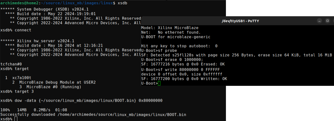
To quickly write to a target DDR2 address from the host for testing, do the following: (1) Program the FPGA bitstream using JTAG, load U-boot into memory, and using Putty break into the U-boot prompt by hitting any key during boot to stop autoboot script.
petalinux-boot jtag --fpga // arg --fpga will flash everything to boot up to U-boot
// In Putty serial session, hit any key to stop autoboot script to get U-boot shell
(2) Use Xilinx System Debugger (XSDB) that is installed with Vivado/Vitis, usable when you source the environment. Connect to the Xilinx Hardware Server, select the Microblaze as a target processor, download data into a specific memory address.
xsdb > connect ; target 3 ; dow -data {~/source/linux_mb/images/linux/BOOT.bin} 0x80000000
(3) Optionally, write memory to the SPI Flash. First erase the entire chip, then program SPI offset 0x0 of size 0x1000000 (16 MB) with data from DDR memory at 0x8000_0000.
U-boot > sf erase 0 1000000 ; sf write 80000000 0 FFFFF0;
Future to-do
- Implement other hardware peripherals on my board, either using Xilinx IP or write my own RTL for SDCard, VGA, Ethernet, USB HID, mono audio out, temperature sensor, and anything else since we have 30 free I/O pins.
- Move to a higher end FPGA that doesn’t limit me to a 16 MB Flash, if I had a 32 MB Flash I wouldn’t need to deal with so many size constaints, a faster system clock (for example, 200 MHz) and improved clock routing resources would also make it easier to meet timing constraints.
- Move Linux kernel and ram-based filesystem to an SD Card, so I wouldn’t need to minimize anything. I would also gain permanent storage for my filesystem. So FPGA bitstream, first stage bootloader, second stage bootloader, would live on SPI Flash only. U-boot would initialize an SD Card controller and load kernel into DDR2 memory from it.